Detailed Hardware Design#
The following sections contain schematic references for PocketBeagle. Full schematics in both PDF and Eagle are available on the ‘PocketBeagle Wiki’
OSD3358-SM SiP Design#
Schematics for the OSD3358-SM SiP are divided into several diagrams.
SiP A OSD3358 SiP System and Power Signals#
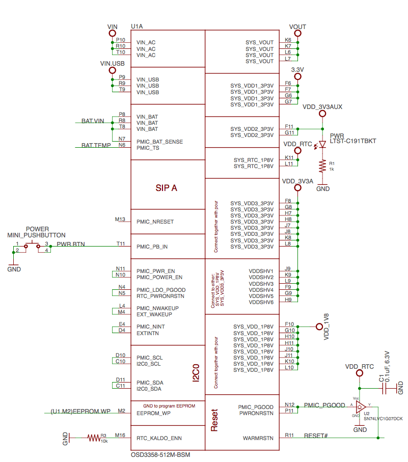
Fig. 296 SiP A OSD3358 SiP System and Power Signals#
SiP B OSD3358 SiP JTAG, USB & Analog Signals#
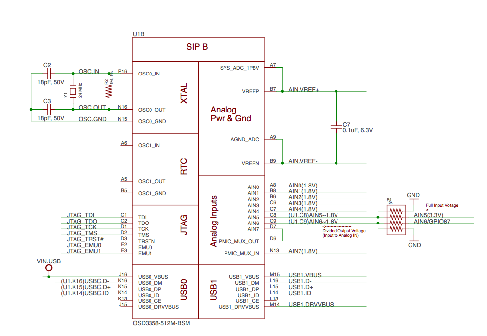
Fig. 297 SiP B OSD3358 SiP JTAG, USB & Analog Signals#
SiP C OSD3358 SiP Peripheral Signals#
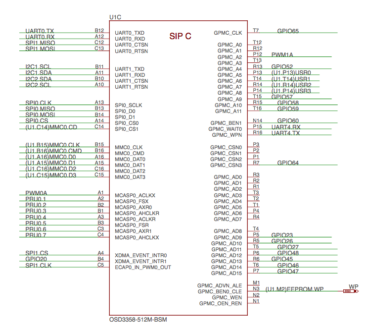
Fig. 298 SiP C OSD3358 SiP Peripheral Signals#
SiP D OSD3358 SiP System Boot Configuration#
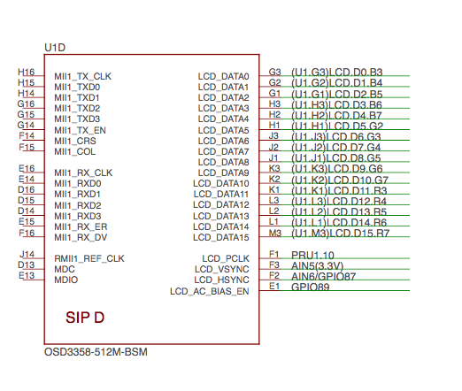
Fig. 299 SiP D OSD3358 SiP System Boot Configuration#
SiP E OSD3358 SiP Power Signals#
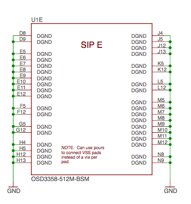
Fig. 300 SiP E OSD3358 SiP Power Signals#
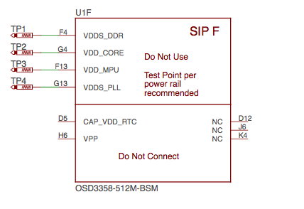
SiP F OSD3358 SiP Power Signals#
MicroSD Connection#
The Micro Secure Digital (microSD) connector design is highlighted in Figure 35.
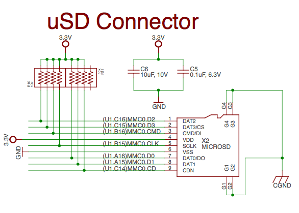
Fig. 301 microSD Connections#
USB Connector#
The USB connector design is highlighted in Figure 36.
Note that there is an ID pin for dual-role (host/client) functionality. The hardware fully supports it, but care should be taken to ensure the kernel in use is either statically or dynamically configured to recognize and utilize the proper mode.
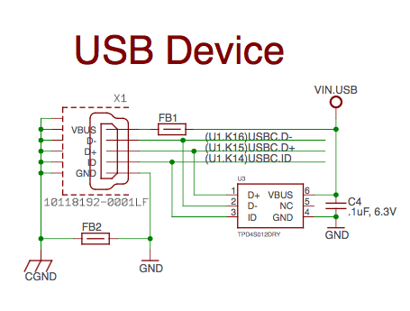
Fig. 302 USB Connection#
User LEDs#
There are four user programmable LEDs on PocketBeagle. The design is highlighted in Figure 38. Table 6 Provides the LED control signals and pins. A logic level of “1” will cause the LEDs to turn on.
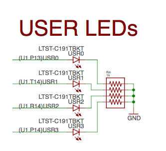
Fig. 304 User LEDs#
LED |
Signal Name |
Proc Ball |
SiP Ball |
USR0 |
GPIO1_21 |
V15 |
P13 |
USR1 |
GPIO1_22 |
U15 |
T14 |
USR2 |
GPIO1_23 |
T15 |
R14 |
USR3 |
GPIO1_24 |
V16 |
P14 |
JTAG Pads#
There are 7 pads on the bottom of PocketBeagle to connect JTAG for debugging. The design is highlighted in Figure 39. More information regarding JTAG debugging can be found at ‘www.ti.com/jtag’
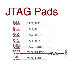
Fig. 305 JTAG Pads Design#
PRU-ICSS#
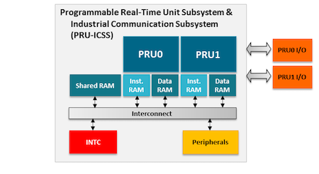
The Programmable Real-Time Unit Subsystem and Industrial Communication SubSystem (PRU-ICSS) module is located inside the AM3358 processor, which is inside the Octavo Systems SiP. Commonly referred to as just the “PRU”, this little subsystem will unleash a lot of performance for you to use in your application. Consisting of dual 32-bit RISC cores (Programmable Real-Time Units, or PRUs), data and instruction memories, internal peripheral modules, and an interrupt controller (INTC). The programmable nature of the PRU-ICSS, along with their access to pins, events and all SoC resources, provides flexibility in implementing fast real-time responses, specialized data handling operations, custom peripheral interfaces, and in offloading tasks from the other processor cores of the system-on-chip (SoC). Access to these pins is provided by PocketBeagle’s expansion headers and is multiplexed with other functions on the board. Access is not provided to all of the available pins.
Some getting started information can be found on https://beagleboard.org/pru.
Additional documentation is located on the Texas Instruments website at processors.wiki.ti.com/index.php/PRU-ICSS and also located at http://github.com/beagleboard/am335x_pru_package.
Example projects using the PRU-ICSS can be found in PRU Cookbook.
PRU-ICSS Features#
The features of the PRU-ICSS include:
Two independent programmable real-time (PRU) cores:
32-Bit Load/Store RISC architecture
8K Byte instruction RAM (2K instructions) per core
8K Bytes data RAM per core
12K Bytes shared RAM
Operating frequency of 200 MHz
PRU operation is little endian similar to ARM processor
All memories within PRU-ICSS support parity
Includes Interrupt Controller for system event handling
Fast I/O interface
– 16 input pins and 16 output pins per PRU core. (Not all of these are accessible on the PocketBeagle. Please check the Pin Table below for PRU-ICSS features available through the P1 and P2 headers.)
PRU-ICSS Block Diagram#
Figure below is a high level block diagram of the PRU-ICSS.
PRU-ICSS Pin Access#
Both PRU 0 and PRU1 are accessible from the expansion headers. Listed below are the ports that can be accessed on each PRU.
Table 6. below shows which PRU-ICSS signals can be accessed on PocketBeagle and on which connector and pins on which they are accessible. Some signals are accessible on the same pins.
Use scroll bar at bottom of chart to see additional features in columns to the right. When printing this document, you will need to print this chart separately.
Header.Pin |
Silkscreen |
Processor Ball |
SiP Ball |
Mode3 |
Mode4 |
Mode5 |
Mode6 |
Note |
|---|---|---|---|---|---|---|---|---|
P1.02 |
A6/87 |
R5 |
F2 |
pr1_pru1_pru_r30_9 (Output) |
pr1_pru1_pru_r31_9 (Input) |
|||
P1.04 |
89 |
R6 |
E1 |
pr1_pru1_pru_r30_11 (Output) |
pr1_pru1_pru_r31_11 (Input) |
|||
P1.06 |
SPI0_CS |
A16 |
A14 |
pr1_uart0_txd (Output) |
UART Transmit Data |
|||
P1.08 |
SPI0_CLK |
A17 |
A13 |
pr1_uart0_cts_n (Input) |
UART Clear to Send |
|||
P1.10 |
SPI0_MISO |
B17 |
B13 |
pr1_uart0_rts_n (Output) |
UART Request to Send |
|||
P1.12 |
SPI0_MOSI |
B16 |
B14 |
pr1_uart0_rxd (Input) |
UART Receive Data |
|||
P1.20 |
20 |
D14 |
B4 |
pr1_pru0_pru_r31_16 (Input) |
||||
P1.26 |
I2C2_SDA |
D18 |
B10 |
pr1_uart0_cts_n (Input) |
UART Clear to Send |
|||
P1.28 |
I2C2_SCL |
D17 |
A10 |
pr1_uart0_rts_n (Output) |
UART Request to Send |
|||
P1.29 |
PRU0_7 |
A14 |
C4 |
pr1_pru0_pru_r30_7 (Output) |
pr1_pru0_pru_r31_7 (Input) |
|||
P1.30 |
U0_TX |
E16 |
B12 |
pr1_pru1_pru_r30_15 (Output) |
pr1_pru1_pru_r31_15 (Input) |
|||
P1.31 |
PRU0_4 |
B12 |
A3 |
pr1_pru0_pru_r30_4 (Output) |
pr1_pru0_pru_r31_4 (Input) |
|||
P1.32 |
U0_RX |
E15 |
A12 |
pr1_pru1_pru_r30_14 (Output) |
pr1_pru1_pru_r31_14 (Input) |
|||
P1.33 |
PRU0_1 |
B13 |
A2 |
pr1_pru0_pru_r30_1 (Output) |
pr1_pru0_pru_r31_1 (Input) |
|||
P1.35 |
P1.10 |
V5 |
F1 |
pr1_pru1_pru_r30_10 (Output) |
pr1_pru1_pru_r31_10 (Input) |
|||
P1.36 |
PWM0A |
A13 |
A1 |
pr1_pru0_pru_r30_0 (Output) |
pr1_pru0_pru_r31_0 (Input) |
|||
P2.09 |
I2C1_SCL |
D15 |
B11 |
pr1_uart0_txd (Output) |
pr1_pru0_pru_r31_16 (Input) |
UART Transmit Data |
||
P2.11 |
I2C1_SDA |
D16 |
A11 |
pr1_uart0_rxd (Input) |
pr1_pru1_pru_r31_16 (Input) |
UART Receive Data |
||
P2.17 |
65 |
V12 |
T7 |
pr1_mdio_mdclk |
MDIO Clk |
|||
P2.18 |
47 |
U13 |
P7 |
pr1_ecap0_ecap_capin_apwm_o |
pr1_pru0_pru_r31_15 (Input) |
Enhanced capture input or Auxiliary PWM out |
||
P2.20 |
64 |
T13 |
R7 |
pr1_mdio_data |
MDIO Data |
|||
P2.22 |
46 |
V13 |
T6 |
pr1_pru0_pru_r31_14 (Input) |
||||
P2.24 |
48 |
T12 |
P6 |
pr1_pru0_pru_r30_14 (Output) |
||||
P2.28 |
PRU0_6 |
D13 |
C3 |
pr1_pru0_pru_r30_6 Output) |
pr1_pru0_pru_r31_6 (Input) |
|||
P2.29 |
SPI1_CLK |
C18 |
C5 |
pr1_ecap0_ecap_capin_apwm_o |
Enhanced capture input or Auxiliary PWM out |
|||
P2.30 |
PRU0_3 |
C12 |
B1 |
pr1_pru0_pru_r30_3 (Output) |
pr1_pru0_pru_r31_3 (Input) |
|||
P2.31 |
SPI1_CS |
A15 |
A4 |
pr1_pru1_pru_r31_16 (Input) |
||||
P2.32 |
PRU0_2 |
D12 |
B2 |
pr1_pru0_pru_r30_2 (Output) |
pr1_pru0_pru_r31_2 (Input) |
|||
P2.33 |
45 |
R12 |
R6 |
pr1_pru0_pru_r30_15 (Output) |
||||
P2.34 |
PRU0_5 |
C13 |
B3 |
pr1_pru0_pru_r30_5 (Output) |
pr1_pru0_pru_r31_5 (Input) |
|||
P2.35 |
A5/86 |
U5 |
F3 |
pr1_pru1_pru_r30_8 (Output) |
pr1_pru1_pru_r31_8 (Input) |
